Light Emitting Ceramic Device And Method


Timeline Photos Electrical Technology Facebook Diodes Electronics Components Light Emitting Diode

Digital Theory Replacement Parts Only Etron Circuit Labs Electronics Basics Electronic Schematics Electronic Engineering

The Salt Crystal Mosaic Ceramic Nightlight Has A Beautiful Mosaic Design Which Adds To The Warmth And Light Of Hima Ceramic Nightlight Salt Crystal Night Light

Hands Down The Best Led Light Therapy Devices Best Seo Services Singapore Cheapest In Singapore Hands D Plaster Wall Lights Led Wall Lights Buy Led Lights

Soberlink Sl2 Medical Device Design Medical Design Devices Design

An organic light emitting display device capable of improving luminance and light extraction efficiency thereof while preventing image blur and a method for manufacturing the same is disclosed.
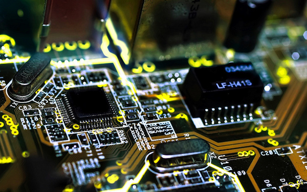
Light emitting ceramic device and method.

Products Hv Ceramic Capacitor Disc Type Detail Spec High Voltage Ceramic Disc Capacitor Doorknob Capacitor Y Capacitors S In 2020 Capacitors High Voltage Resistors

White Light Emitting Diodes History Progress And Future Cho 2017 Laser Amp Photonics Reviews Wiley Online Library

What Is Capacitor Types Formula Symbol How It Works Unit Capacitors Electronic Engineering Rc Time Constant

Blue Light Emitting Ceramic Nano Pigments Of Tm3 Doped Yalo3 Applications In Latent Finger Print Anti Counterfeiting And Porcelain Stoneware Sciencedirect

General Information For Ceramic Capacitors Capacitors Ceramics Ceramic Materials

Source Designboom Com 3dprinting Design Industrial Design Trends Design
Ceramics And Glass In Electrical And Electronic Applications The American Ceramic Society Electroceramics Electronic Devices

Amazon Com Sun System Grow Lights Lec 630w 120v 3100k Lamps Indoor Grow Light Fixture For Hydroponic And Greenhouse Use Philips Green Power Full Spectrum Cdm Lamps And

Samsung Galaxy S10 Pre Orders In China Make A Strong Start Samsung Galaxy Galaxy Samsung

Pin On Crystal Substrates

Steam Table Lamp Designer Rikke Hagen Scandinavian Lamps Modern Light Fixtures Lamp

3 Ring Bdc Pro 3 5ml Atomizer By Iciga 16 50 Vape95 Com I Want This Ceramic Coil Self Cleaning Charcoal Filter It S Cheap T With Images Vape Addict Vape Color Ring

Amazon Com Ceramic Heat Emitter Reptile Heat Lamp 100 Watt Lizard Heat Lamp Bulb No Light Emitting Snake Lizard Gecko Turtle Snake Lizard Gecko Turtle Brooder Chick Coop Heater 2 Pack Black Home

Do You Know The Three Methods To Produce Gallium Arsenide Wafers Read About It In Our Blog Wafer Blog Method

Alternative Replacement Cross Reference For Murata High Voltage Lead Type And Screw Terminal Type Ceramic Capacitor High Voltage Capacitors Lead Type

How To Fix A Broken Flat Screen Lcd Led Tv With Lines Or Cracks Led Tv Screen Repair Broken Screen

An Adjustable Track Style Ceiling Fixture With Bronze Finish And Energy Efficient Leds Svetilniki

Artificial Neurons On Silicon Chips That Behave Just Like The Real Thing Have Been Invented By Scientists A First Of I Semiconductor Medical Device Electronics

Sun System Flower Power 315 Watt Lec Fixture 120 240 Volt 315 Watt Cmh Grow Lights Ceramic Grow Lights Grow Lights

Uniform Nanowire Arrays For Science And Manufacturing Science Materials Science Material Science

Top 2019 Best Led Grow Light Reviews 420 Green Thumb Led Grow Lights Best Led Grow Lights Grow Lights

The Indoor Barking Dog Deterrent Hammacher Schlemmer Dog Deterrent Dog Bark Control Pet Safe

Mybat Tuff Hybrid M Stand Case For Galaxy Light T399 Black Black Wow Galaxy Lights Silicone Cover Galaxy

Amazon Com Mudder 45w 225 Led 2835smd Plant Grow Red Blue Light Square Shape Panel Lamp With Us Plug For Grow Lights For Plants Indoor Flowers Grow Lights

Piezoelectric Technology Leading The New Technological Era Green Energy Drink Mechanical Energy Energy Transformations

Calla Jewel Wall Light In Brass White Design Monzer Hammoud Pont Des Arts Studio Paris Sculpture Art Brass Wal White Wall Lights Lamp Design Wall Lamp

Be Creative Mary Pottery Pottery Ceramic Cups Tea Bowls

Insulator Seal Isi A Division Of Mdc Vacuum Products Offers A Complete Line Of Viewports For All Of Your Visual Optical And Broad Brazing Vacuums Optical

Common Capacitor Types In 2020 Capacitors Diy Electronics Electronics Projects Diy

Mcs Es Accommodation Resources Assistive Devices Personal Protective Equipment Assistive Technology

Merder House Of Candles Grey S Anatomy Phone Case By Megan Roberts Greys Anatomy Phone Cases Greys Anatomy Gifts Greys Anatomy

W5w 168 194 921 T10 Leds Led Led Lights Led Bulb

Birch Lane Heritage Pedra 38 5 Table Lamp Table Lamp Table Lamp Sets Butler Table

Laser Hair Removal In 2020 Laser Hair Removal Ipl Laser Hair Removal Laser Hair Removal Machine

Conquest S12 Price Specifications Features View Cell Phone Specials Best Mobile Phone Compare Phones

Pureglow Crystal 2 In 1 Himalayan Salt Lamp Ultrasonic Essential Oil Diffuser Patent Pending Himalayan Salt Lamp Salt Rock Lamp Pure Products

Silkn Glide Ipl Hair Remover Laser Hair Removal Epilator 150000 Pulses Permanent Hair Removal Device V Hair Removal Permanent Hair Removal Devices Hair Removal

Pin On Ultrasonic Pest Repeller

Pin On Best Essential Oil Diffuser To Cure Insomnia

Plantui Smart Garden 6 Grey Smart Garden Garden Design Soil

Stretchable Transparent Heater Made From Metallic Glass Wearable Electronics Transparent Metal

Resistor Types Of Resistors Fixed Variable Linear Non Linear Resistors Electronics Basics Diy Electronics
Source : pinterest.com
